Spin coating technology is an important method for producing thin films on flat surfaces through controlled rotation and liquid spreading. It is widely used in semiconductor research, materials science, microfabrication, nanotechnology, and the development of advanced electronic materials. The process involves placing a liquid solution on a substrate and rotating it at a selected speed so that the liquid spreads across the surface. As the solvent evaporates, a thin layer of the remaining material forms.
Thin films are essential in many modern technologies because they can modify the electrical, optical, chemical, and mechanical properties of a surface. Spin coating provides researchers with a practical way to prepare these layers and investigate how processing conditions influence their performance. Although the method is relatively straightforward, producing a consistent film requires careful control of solution properties, substrate preparation, rotational speed, and drying conditions.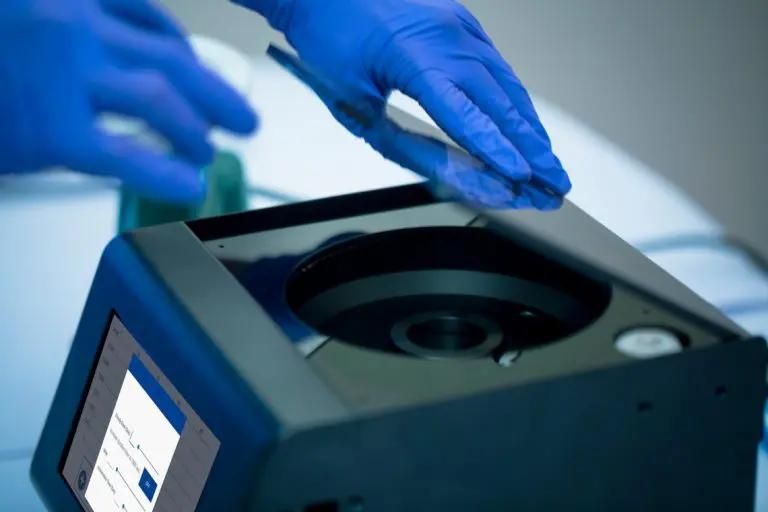
What Is Spin Coating Technology?
Definition of Spin Coating
Spin coating is a thin-film deposition technique that uses rotational motion to distribute a liquid coating material across a substrate. The substrate is typically a flat piece of silicon, glass, polymer, or another compatible material. A measured quantity of solution is placed on the surface, and the substrate rotates to spread the liquid while excess material moves toward the edges.
The liquid layer becomes progressively thinner as it spreads and loses solvent. Depending on the formulation, the remaining material may form a polymer film, photoresist layer, functional coating, or another solid layer. Researchers use spin coating because its operating parameters can be adjusted to investigate film thickness, uniformity, and surface characteristics.
Important Facts About Thin Films
Thin films are layers of material whose thickness is small compared with their lateral dimensions. Their properties can differ from those of the same material in bulk form because thickness, surface structure, molecular arrangement, and interfaces can influence material behaviour. In electronics, for example, a thin layer may function as an insulating film, an active semiconductor layer, or a light-sensitive coating.
Film thickness is often measured in nanometres or micrometres, depending on the application. A nanometre is one-billionth of a metre, while a micrometre is one-millionth of a metre. The appropriate thickness depends on the material and its intended function, so spin coating does not produce one universal film thickness.
How the Spin Coating Process Works
Substrate Preparation
The first stage of spin coating involves preparing the substrate. Dust, oils, moisture, and other contaminants can interfere with liquid spreading and film adhesion. Researchers therefore select suitable cleaning and surface preparation procedures based on the substrate material and the chemical properties of the coating solution.
Surface energy and roughness also influence the way a liquid interacts with the substrate. A solution may spread easily on one surface but form droplets or uncovered areas on another. Proper preparation helps improve wetting and makes it easier to produce repeatable experimental results.
Solution Dispensing and Rotation
After substrate preparation, the coating solution is dispensed onto the surface. The amount of solution depends on the substrate size, formulation, and process requirements. The substrate then rotates at a controlled speed, causing the liquid to spread outward while excess solution leaves the surface.
Some procedures dispense the solution before rotation begins, while others introduce it during the initial spinning stage. The appropriate method depends on the coating material and the desired coverage. Rotational speed, acceleration, and spinning duration are important variables because they influence the movement of the liquid during film formation.
Solvent Evaporation and Final Film Formation
During rotation, the solvent gradually evaporates, increasing the concentration of the material remaining on the substrate. As the liquid becomes more concentrated, its flow characteristics change and a solid or semi-solid layer begins to form. The evaporation rate depends on solvent volatility, temperature, airflow, humidity, and the composition of the coating solution.
Some materials require additional drying, heating, or curing after spinning. These steps can help remove residual solvent or establish the intended film properties. The required conditions vary with the chemistry of the coating and the temperature tolerance of the substrate.
Key Spin Coating Technology Facts About Film Thickness
The Effect of Rotational Speed
Rotational speed is one of the most influential parameters in conventional spin coating. Under many comparable processing conditions, a higher spinning speed produces a thinner film because more liquid is removed from the substrate. However, the relationship is affected by solution viscosity, evaporation rate, material concentration, and the timing of the spinning stages.
The relationship between speed and thickness is not identical for every material. A process developed for one polymer or photoresist may not produce the same result with a different formulation. Researchers therefore use controlled experiments to identify suitable operating conditions for each coating system.
The Importance of Solution Viscosity
Viscosity describes how strongly a liquid resists flowing. A higher-viscosity solution may retain more material on the substrate under otherwise similar conditions, while a lower-viscosity solution may spread more readily. Nevertheless, viscosity interacts with other variables, so film thickness cannot be predicted from viscosity alone.
Temperature, solvent composition, polymer concentration, and molecular characteristics can influence viscosity. Consistent preparation and handling of the solution help researchers reduce variation between experiments and compare results more reliably.
The Role of Solvent Evaporation
Solvent evaporation influences both liquid movement and the transition from a flowing solution to a solid film. If evaporation occurs rapidly, the material may become concentrated before the liquid has fully levelled. Slower evaporation may allow more time for spreading but can extend drying time or affect the final material structure.
The choice of solvent is therefore an important part of thin-film process development. Researchers consider solubility, volatility, material compatibility, safety, and the desired final film properties when selecting a formulation.
Materials Commonly Used in Spin Coating
Polymer Thin Films
Polymer solutions are widely used in spin coating because many polymers can be dissolved in suitable solvents and deposited as thin layers. Depending on their composition, these films can be used in flexible electronics, protective coatings, membranes, sensors, and laboratory materials research.
The properties of a polymer film depend on its molecular characteristics, solution concentration, solvent selection, and drying conditions. Researchers may also investigate how processing affects film smoothness, adhesion, mechanical behaviour, and stability.
Photoresists for Semiconductor Processing
Photoresists are light-sensitive materials used in photolithography to transfer patterns onto substrates. Spin coating is commonly used to apply photoresist to silicon wafers and other compatible surfaces before exposure and development. The thickness and uniformity of the resist layer can affect the quality of the resulting pattern.
Semiconductor research requires carefully controlled coating conditions because defects or thickness variations can influence later processing stages. The selected spin speed and baking conditions depend on the photoresist formulation, substrate dimensions, and intended lithography process.
Organic Electronic Materials
Spin coating is used in research involving organic semiconductors, conductive polymers, and other solution-processable electronic materials. These materials are investigated for applications such as organic light-emitting diodes, organic photovoltaic cells, and flexible electronic devices.
The arrangement of molecules within a thin film can influence electrical and optical behaviour. Solvent evaporation, material concentration, and drying conditions may therefore affect the performance of experimental devices. Each formulation requires its own process evaluation because different materials respond differently to the same operating conditions.
Applications of Spin Coating Technology
Semiconductor Manufacturing and Microfabrication
Spin coating is particularly important in semiconductor processing research, where thin layers are required for lithography, insulation, and experimental device structures. Photoresist coating is a prominent example because uniform coverage supports accurate pattern transfer. Researchers also investigate spin-coated polymer layers and other solution-based materials used in microfabrication.
The method is useful for preparing samples under controlled conditions and evaluating how coating parameters affect device fabrication. However, semiconductor manufacturing also requires contamination control, precise equipment operation, and compatibility with the wider production process.
Solar Cell and Renewable Energy Research
Spin coating is used in laboratory research on solution-processable photovoltaic materials. Depending on the device architecture, it may be used to deposit active layers, charge-transport layers, or intermediate coatings. These layers influence how light is absorbed and how electrical charges move through the device.
Researchers examine film uniformity, surface morphology, and material composition to understand their relationship with photovoltaic performance. Moving from laboratory samples to large-scale production can introduce additional challenges involving material consumption, coating speed, substrate size, and process consistency.
Optical Coatings and Photonics
Thin films are important in optical technologies because they can influence how light is transmitted, reflected, absorbed, or scattered. Spin coating allows researchers to prepare selected solution-based optical materials on glass and other compatible substrates.
The optical response of a film depends on its thickness, refractive index, composition, and surface quality. Researchers may use spin coating to study these relationships in optical sensors, photonic materials, and experimental coating systems. Applications requiring highly precise multilayer structures may need additional deposition techniques.
Sensors and Advanced Materials Research
Spin-coated layers can be used in the development of chemical sensors, environmental sensors, and other experimental sensing devices. Depending on the material, a thin film may provide a functional surface, control interactions with the surrounding environment, or contribute to the electrical response of a sensor.
Materials scientists also use spin coating to investigate polymer interfaces, surface treatments, and nanoscale structures. The technique offers a practical way to prepare small samples for controlled experiments, although the final properties must be confirmed through appropriate measurements.
Advantages and Limitations of Spin Coating
Main Advantages
One major advantage of spin coating is its relatively simple operating principle. A suitable spin coater can spread a solution across a flat substrate while allowing the operator to adjust speed, acceleration, and duration. This makes the technique useful for research that involves repeated experiments and comparisons between different formulations.
Spin coating also supports a range of solution-processable materials. Researchers can investigate polymers, photoresists, organic electronic materials, and selected functional coatings without necessarily requiring the specialised equipment used for some vapour-based deposition processes.
Common Limitations
Spin coating is less suitable for certain complex or irregular surfaces because the liquid tends to spread outward across the rotating substrate. Much of the dispensed solution may also leave the substrate, which can increase material waste. These limitations can become significant when using expensive materials or preparing large-area coatings.
Film quality can also be affected by edge beads, poor wetting, pinholes, contamination, and uneven solvent evaporation. Careful process control and suitable measurement methods are needed to identify and reduce these defects. Other coating technologies may be more appropriate when material efficiency, substrate shape, or large-scale production is the primary concern.
Equipment Used in Spin Coating Research
Laboratory Spin Coater
A laboratory spin coater is designed to rotate a substrate at a selected speed. Depending on the model, it may include programmable speed settings, adjustable acceleration, timed processing stages, a sample holder, and a protective enclosure. Some systems are designed for small research samples, while others accommodate larger substrates or specialised experimental setups.
The appropriate equipment depends on substrate size, chemical compatibility, required speed range, process repeatability, and laboratory safety needs. Equipment selection should also account for the coating materials and solvents used during the process.
Thin-Film Characterisation Instruments
Producing a film is only one part of thin-film research. Researchers also need to measure its thickness, surface quality, composition, and other relevant properties. Profilometry can measure surface height differences, while ellipsometry can estimate thin-film thickness and optical properties under suitable conditions.
Optical microscopy and other surface-characterisation techniques may help identify defects or uneven coverage. The correct measurement method depends on the material, expected thickness, substrate, and experimental objective. Combining process records with measurement results helps researchers understand which parameters have the greatest influence on film quality.
Quality Control and Safety in Spin Coating
Improving Film Uniformity
Film uniformity depends on the consistency of the substrate, solution, dispensing process, rotational profile, and drying conditions. Researchers can improve repeatability by standardising preparation procedures and documenting the settings used for each sample. Measuring several locations across a film can help identify thickness variations that may not be visible during ordinary inspection.
Changing one process variable at a time can make troubleshooting more systematic. For example, researchers may compare different rotational speeds while keeping the solution composition and substrate preparation constant. This approach helps identify relationships between processing conditions and measured film characteristics.
Chemical and Equipment Safety
Spin coating solutions may contain volatile, flammable, or otherwise hazardous solvents. Before use, laboratory personnel should review the relevant safety data sheets and follow established procedures for ventilation, protective equipment, chemical storage, and waste disposal. Used solutions should be handled according to laboratory rules and applicable environmental requirements.
The rotating substrate must also be secured properly, and the equipment should be operated according to the manufacturer's instructions. Operators should not interfere with moving components while the system is running. Regular inspection and suitable training help support safe operation and consistent research results.
Frequently Asked Questions About Spin Coating Technology
What Is the Main Purpose of Spin Coating?
The main purpose of spin coating is to deposit a relatively uniform thin layer of material on a suitable substrate. It is widely used in semiconductor research, photoresist processing, polymer films, organic electronics, and laboratory materials development.
What Factors Affect Spin-Coated Film Thickness?
Important factors include rotational speed, solution viscosity, material concentration, solvent volatility, substrate properties, dispensing conditions, and environmental factors. Their combined effects determine the thickness and uniformity of the resulting film.
Why Is Spin Coating Used in Semiconductor Research?
Spin coating is commonly used to deposit photoresists and selected solution-based materials onto wafers and other flat substrates. Uniform layers help support photolithography, experimental device fabrication, and the investigation of thin-film properties.
Can Spin Coating Be Used for Nanotechnology Research?
Yes. Spin coating is used to prepare polymer films, organic electronic layers, and other functional coatings for laboratory-scale nanotechnology studies. The technique is particularly useful when the material can be processed from a suitable solution.
How Is Spin-Coated Film Quality Evaluated?
Film quality can be evaluated through thickness measurements, surface inspection, microscopy, and other material-characterisation techniques. The selected method depends on the film's properties and the requirements of the research.
Conclusion
Spin coating technology provides a practical method for forming thin films in semiconductor research, microfabrication, materials science, renewable energy studies, and advanced coating development. The process relies on controlled rotation, liquid spreading, and solvent evaporation, with the final film properties influenced by material composition and operating conditions.
Understanding rotational speed, viscosity, solvent behaviour, substrate preparation, and drying conditions helps researchers improve process consistency. Although spin coating has limitations involving material waste, substrate geometry, and sensitivity to process conditions, it remains useful for preparing and studying solution-based thin films. Combining controlled deposition with suitable characterisation, careful documentation, and laboratory safety procedures supports reliable research and the development of advanced materials.