
Automatic wafer dicing systems are precision machines used to separate individual semiconductor chips, commonly known as dies, from a processed silicon wafer. These systems are an important part of semiconductor manufacturing because integrated circuits are typically fabricated in large numbers on a single wafer before being separated for packaging and testing.
During semiconductor production, a wafer passes through several processes, including deposition, lithography, etching, doping, and metallization. These steps create electronic circuits on the wafer surface. Once fabrication and the required inspection stages are complete, the wafer is divided into individual dies using a suitable dicing technology.
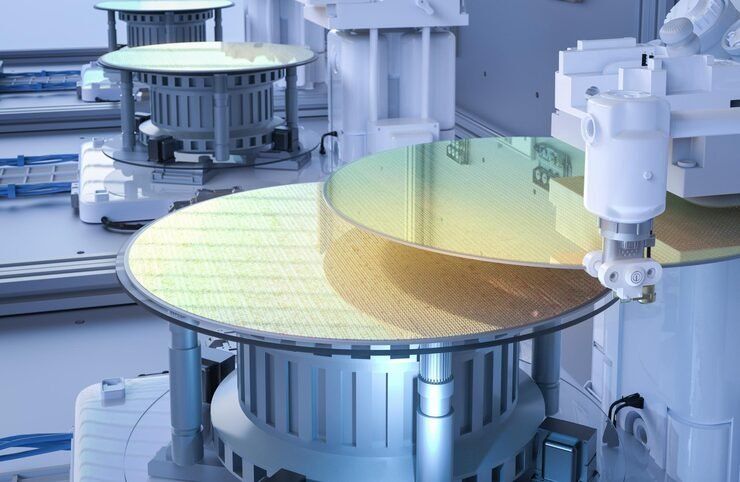
Automatic wafer dicing equipment combines precision positioning, controlled cutting or separation, wafer handling, and inspection functions. Depending on the design, the equipment may use a rotating blade, a laser, plasma etching, or another specialized technique to separate the dies while limiting damage to delicate structures.
Why wafer dicing is important
Semiconductor wafers contain numerous individual circuits arranged in a grid. The spaces between these circuits, known as streets or dicing lanes, provide the intended paths for separation. Accurate alignment with these lanes helps prevent damage to the active circuit areas.
Wafer dicing is particularly important because modern semiconductor devices may contain very small features, thin substrates, and fragile structures. An unsuitable cutting process can cause chipping, cracking, contamination, or damage to sensitive layers.
Automatic systems help maintain repeatable movement and controlled processing conditions. They are used in the production of microprocessors, memory chips, power semiconductors, sensors, optical devices, and other electronic components.
Main components of an automatic wafer dicing system
A typical system may contain several integrated components:
Wafer holding mechanism: Secures the wafer or wafer tape during processing.
Precision positioning stage: Moves the wafer accurately along the required cutting paths.
Dicing tool: Uses a blade, laser, plasma process, or another separation method.
Optical alignment system: Identifies wafer features and aligns the cutting paths.
Process control system: Manages movement, cutting parameters, and operating sequences.
Cooling and debris management: Helps control heat, remove particles, or manage process residue where required.
Inspection system: Checks alignment, edge quality, and visible defects in applicable configurations.
The exact configuration depends on the wafer material, die dimensions, substrate thickness, production volume, and required edge quality.
Importance of Automatic Wafer Dicing in Semiconductor Manufacturing
Wafer dicing is a critical transition between wafer fabrication and semiconductor packaging. The quality of this process affects die dimensions, edge integrity, material yield, and the reliability of downstream assembly operations.
As semiconductor devices become smaller and more complex, manufacturers must manage increasingly demanding requirements for cutting accuracy and substrate handling. Automatic wafer dicing systems help control these operations through programmable movement, optical alignment, and repeatable process settings.
Semiconductor applications
Automatic wafer dicing equipment is used across several areas of electronics manufacturing.
Integrated circuits: Separates dies containing logic, computing, and control circuits.
Memory devices: Processes wafers used to manufacture memory chips.
Power semiconductors: Separates devices used in power conversion, electric vehicles, and industrial electronics.
Microelectromechanical systems (MEMS): Processes wafers containing miniature mechanical structures, sensors, and actuators.
Optical semiconductors: Separates laser devices, photodetectors, and other optoelectronic components.
Radio-frequency devices: Processes specialized semiconductor components used in wireless communication systems.
Compound semiconductors: Handles materials such as gallium arsenide, silicon carbide, and gallium nitride, subject to their specific processing requirements.
Different applications require different dicing methods. A silicon logic wafer may be suitable for conventional blade dicing, while a thin wafer or a material that is sensitive to mechanical stress may require laser-based or another specialized separation process.
Challenges addressed by automated dicing
Automation helps manufacturers manage several recurring production challenges.
Cutting accuracy: Precision stages and alignment systems help follow the designated dicing lanes and maintain the intended die dimensions.
Material damage: Appropriate tool selection, cutting parameters, and wafer support can reduce chipping, cracking, and other forms of damage.
Production consistency: Programmable recipes help maintain repeatable operating conditions across multiple wafers.
Contamination control: Cooling arrangements, filtration, cleaning procedures, and controlled material handling help manage particles and process residue.
Thin-wafer handling: Specialized supports and tape systems help stabilize wafers that may be difficult to handle because of their reduced thickness.
Automation does not eliminate every source of defects. Wafer quality, cutting-tool condition, material properties, alignment accuracy, and process settings all influence the final result.
Conventional and automated wafer dicing
Feature | Manual or basic equipment | Automatic wafer dicing system |
|---|---|---|
Alignment | May require substantial operator input | Can use automated optical alignment |
Movement | Depends on equipment configuration | Programmable precision stages |
Process control | May involve manual adjustments | Recipe-based control and monitoring |
Production records | May require separate documentation | Can support digital process records |
Inspection | Often performed separately | May include integrated inspection functions |
Application | Limited or specialized production tasks | Repetitive, controlled wafer processing |
The distinction depends on the equipment design. Not every automatic machine includes integrated inspection or advanced data collection, and manual oversight remains important in semiconductor production.
Recent Developments in Wafer Dicing Technology
Developments during 2024–2026 have focused on processing thinner wafers, improving die separation, managing increasingly diverse semiconductor materials, and integrating dicing with advanced packaging workflows. These trends reflect the changing requirements of computing, automotive electronics, power conversion, and high-density electronic assemblies.
Laser dicing and low-damage processing
Laser dicing uses focused laser energy to modify or separate material along defined paths. Depending on the technique, the laser may ablate material, create internal modifications, or assist separation through a combination of laser processing and mechanical action.
Stealth dicing is one approach in which laser energy creates modified regions inside a suitable wafer, allowing the material to separate along planned lines. Because the process can reduce direct mechanical contact at the wafer surface, it is relevant to certain thin-wafer and specialized semiconductor applications.
Laser-based processes are not universally suitable. Material absorption, wafer structure, thermal effects, surface coatings, and the required edge quality influence whether a particular technique can be used.
Advanced packaging and thinner wafers
Semiconductor packaging increasingly uses approaches such as chiplets, stacked dies, and three-dimensional integration. These architectures can involve thin dies and materials with different mechanical characteristics, increasing the importance of precise separation and careful handling.
Dicing systems may therefore be configured to work with temporary bonding materials, protective films, specialized tapes, and thin-wafer support arrangements. The objective is to preserve the integrity of each die for subsequent assembly.
Process monitoring and automation
Modern wafer dicing equipment may combine optical cameras, automated alignment, recipe management, and equipment monitoring. Some systems can record process parameters and inspection information to help engineers identify recurring defects or changes in cutting performance.
Data integration can also support traceability between wafer identification, processing conditions, and downstream inspection results. The degree of automation varies by machine and production environment.
Material-specific dicing methods
Silicon remains widely used, but semiconductor manufacturing also relies on materials such as silicon carbide, gallium nitride, and gallium arsenide. These materials differ in hardness, brittleness, thermal behavior, and response to cutting or laser energy.
Consequently, the same dicing parameters cannot be applied to every wafer. Equipment selection and process development must account for the substrate, wafer thickness, device layout, and acceptable damage limits.
Laws, Standards, and Semiconductor Manufacturing Requirements
Automatic wafer dicing systems operate within a broader framework of semiconductor manufacturing standards, workplace safety requirements, equipment regulations, and environmental controls. The applicable requirements depend on the manufacturing location, equipment configuration, and materials being processed.
Semiconductor equipment standards
Several standards and technical frameworks are relevant to semiconductor equipment and manufacturing environments.
SEMI standards: The Semiconductor Equipment and Materials International standards framework includes technical requirements and guidance covering semiconductor manufacturing equipment, safety, materials, and facility-related practices.
ISO 9001: Establishes requirements for quality management systems that can support consistent equipment manufacturing and production controls.
ISO 14644: Addresses cleanroom classification and related contamination-control requirements.
IEC 60204-1: Covers electrical equipment of machinery, including relevant electrical safety requirements.
ISO 12100: Provides principles for machinery risk assessment and risk reduction.
The applicability of an individual standard depends on the equipment and the jurisdiction. Compliance with one standard does not automatically establish compliance with all relevant regulations.
Safety and environmental considerations
Wafer dicing can involve rotating blades, high-speed moving stages, lasers, electrical systems, cooling liquids, and fine process particles. Equipment designs and operating procedures must address the hazards associated with the specific dicing method.
Laser-based equipment may require protective enclosures, interlocks, and controls appropriate to the laser classification. Mechanical dicing systems require safeguards against contact with moving parts and exposure to process fluids.
Environmental controls can include the collection and treatment of used cutting water, management of suspended particles, appropriate chemical handling, and disposal of process waste according to applicable rules. Facilities must also consider ventilation, electrical safety, and worker training.
Requirements in India and international markets
In India, semiconductor equipment installations may be subject to applicable factory safety requirements, electrical regulations, environmental rules, and relevant product or machinery standards. The specific obligations depend on the facility and the equipment involved.
International manufacturing sites may also need to consider regional machinery, workplace safety, and environmental requirements. Semiconductor manufacturers frequently use internal qualification procedures and customer specifications in addition to applicable legal requirements.
Tools and Resources for Wafer Dicing
Selecting a wafer dicing system requires technical information about the substrate, die layout, production volume, and downstream assembly process. Equipment specifications alone are not sufficient to determine whether a particular method will produce acceptable results.
Important equipment and process tools
Wafer mapping and alignment systems: Optical cameras and pattern-recognition software identify wafer features and establish cutting coordinates.
Precision motion stages: Controlled positioning systems move wafers or cutting heads along programmed paths.
Dicing blades: Precision blades are selected according to the substrate, required kerf width, cutting depth, and surface-quality requirements.
Laser processing systems: Focused laser equipment performs material ablation, internal modification, or other specialized separation processes.
Inspection and metrology systems: Optical microscopes and automated imaging tools examine die edges, cracks, chipping, alignment, and other visible defects.
Process monitoring software: Records recipes, operating parameters, equipment status, and inspection data where these functions are supported.
Factors to consider when selecting equipment
Selection factor | Technical importance |
|---|---|
Wafer material | Determines suitable cutting or separation technologies |
Wafer thickness | Influences support, handling, and process parameters |
Die dimensions | Affects cutting-path layout and positioning requirements |
Kerf width | Determines the material removed between adjacent dies |
Edge quality | Influences acceptable chipping and damage limits |
Production volume | Affects automation and throughput requirements |
Contamination control | Determines cleaning, filtration, and handling needs |
Integration requirements | Affects compatibility with wafer mounting, inspection, and packaging equipment |
Common manufacturing and quality-control stages
Wafer dicing typically begins with wafer identification and inspection. The wafer may then be mounted on dicing tape or another suitable support before alignment and cutting.
During processing, the machine follows programmed dicing paths using the selected blade or laser technique. After separation, the dies may undergo cleaning, inspection, and handling procedures before moving to die bonding or other packaging stages.
Quality checks may examine dimensional accuracy, edge damage, die separation, contamination, and the condition of sensitive device structures. Process records help link inspection findings to the corresponding wafer and production conditions.
Frequently Asked Questions
What is an automatic wafer dicing system?
An automatic wafer dicing system is a precision machine that separates a processed semiconductor wafer into individual dies using a controlled cutting or separation technique. It typically incorporates wafer handling, alignment, motion control, and process monitoring.
What is the difference between blade dicing and laser dicing?
Blade dicing uses a rotating precision blade to cut through the wafer, while laser dicing uses focused laser energy to remove or modify material along planned paths. The appropriate method depends on the substrate, thickness, device structure, and edge-quality requirements.
Which materials can wafer dicing machines process?
Depending on their configuration, wafer dicing machines can process silicon, silicon carbide, gallium arsenide, gallium nitride, and certain other semiconductor materials. Each material may require different tools, processing parameters, and handling arrangements.
Why is precision important in semiconductor wafer dicing?
Precision helps maintain die dimensions and alignment while limiting damage to active circuit regions. It also supports consistent separation, inspection, and downstream semiconductor packaging.
What affects the selection of wafer dicing equipment?
Important factors include wafer material, thickness, die size, kerf width, required edge quality, production volume, contamination controls, and compatibility with other manufacturing equipment.
Conclusion
Automatic wafer dicing systems separate processed semiconductor wafers into individual dies for subsequent packaging and testing. Blade dicing, laser-based techniques, and other specialized approaches address different material and manufacturing requirements. Equipment performance depends on precision alignment, controlled processing, wafer handling, inspection, and contamination management. Advances in thin-wafer processing, advanced packaging, and digital monitoring continue to shape semiconductor dicing technology.